Optical Metrology
Enabling technologies and subsystems for 3D surface measurement
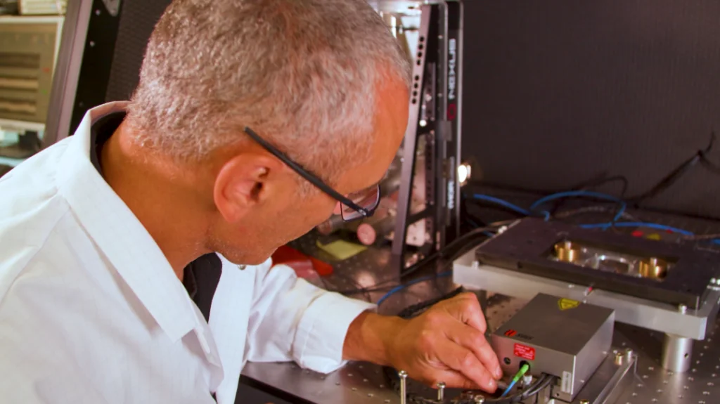
Optical metrology relies on high-performance movement coupled with high-quality optics. The technique is often used for quality control and inspection of components and plays a critical role in many modern manufacturing processes.
Different microscopes and microscopy techniques provide a range of optical metrology methods, offering a range of resolutions for various applications.
Surface analysis
High-resolution measurements of roughness or waviness are essential for quality control in manufacturing semiconductor wafers. Confocal microscopy and white light interferometry are both non-contact, optical metrology methods that achieve low-nanometer resolution of surface profiles.
Atomic force microscopy (AFM) and scanning, electron microscopy are alternative, non-optical methods, that also give sub-nanometer resolution of surface profiles but are not suited to all sample types.
3D measurement
A conventional, automated microscope, can produce topographic profiles of objects with low micron resolution using the confocal technique.
Feature identification
At lower resolutions, imaging methods can greatly impact the quality of measurements. Darkfield illumination or differential interference contrast (DIC) can identify specific features not easily identified using standard brightfield microscopy.
Positioning accuracy and motion control
While imaging techniques vary, motion control is a crucial part of any optical metrology system. For high-resolution measurements, where motion control accuracy down to picometers is needed, low electronic noise is essential. Queensgate’s piezo nanopositioning stages combine low-noise electronics with capacitive sensors to provide measurement resolution down to 0.2 nm. Response time below 1 ms together with world-leading velocity control enable image collection at speeds greater than 1000 µm/s.
NPS-Z-250B high load 250 µm piezo stage with capacitive sensor
6 kg payload as standard, provides 250 µm travel and, with flexure guidance and capacitive sensors, offers the highest precision positioning.
NPS-X-60/100D High load direct nanopositioning stages
Maximum payload up to 10 kg, fast response time to provide optimal performance in demanding high-speed, high-precision applications such as optical metrology.
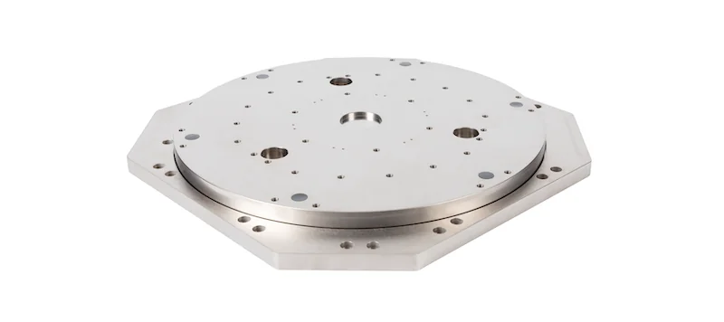
WP120A wafer positioner/scanner
The stage is designed to hold 300 mm (12″) wafers and delivers exceptional performance with loads of up to 8 kg suitable for heavy wafer chucks.
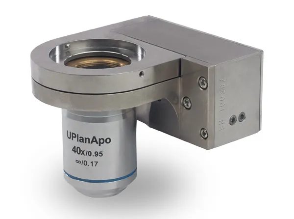
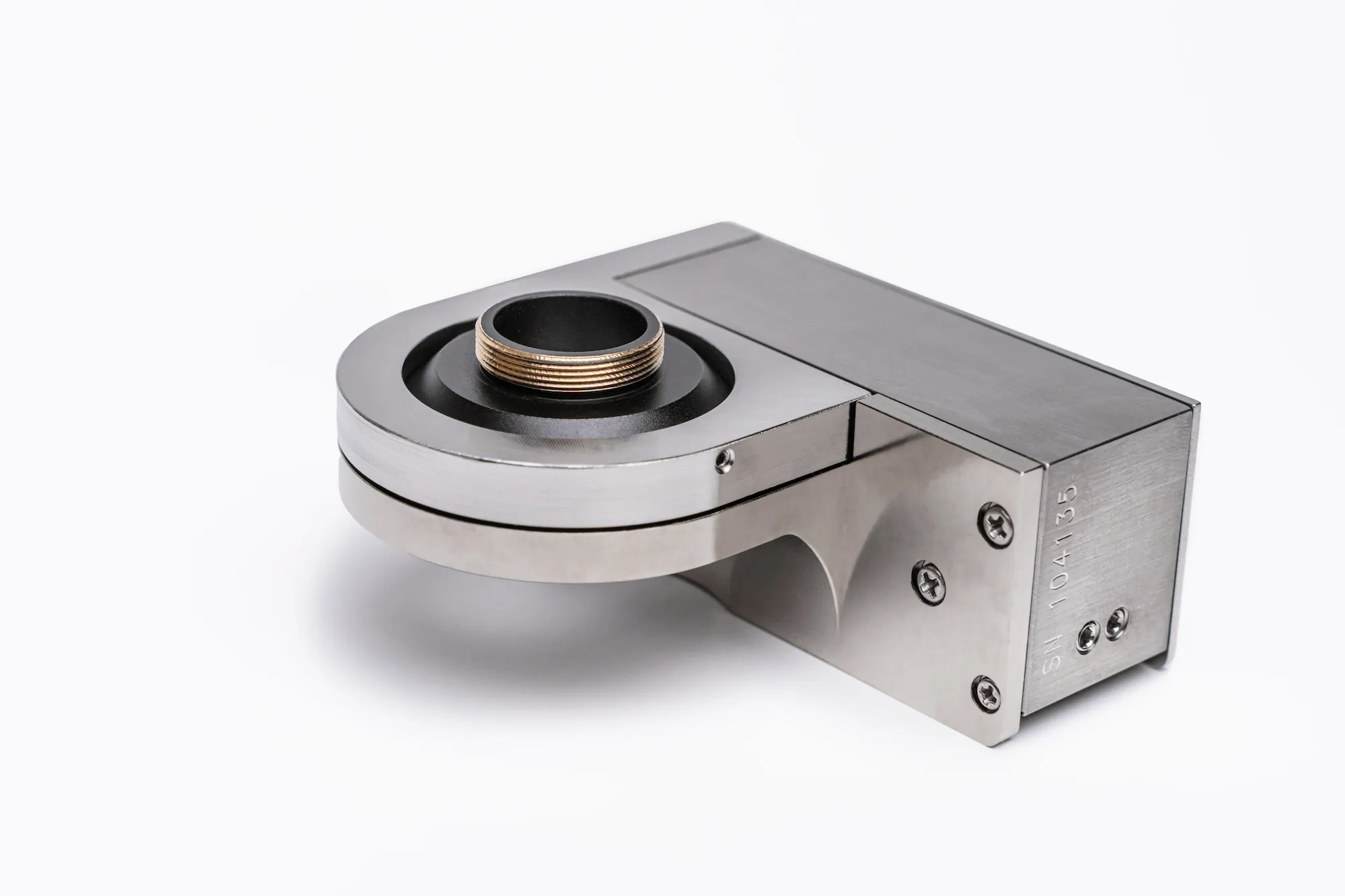
NanoScan OP800 Objective Positioner/Scanner with 800 µm range
The OP800 provides the fastest step and settle time of any piezo-driven objective positioner. It features capacitive feedback sensors that ensure exceptional repeatability and resolution. 400 µm and 200 µm versions available.
Prior Scientific offers a range of components for applications in optical metrology
The ProScan H112 motorized 12-inch travel stage and control electronics ensure accuracy and repeatability suitable for optical metrology applications with sub-micron resolution.
Real-time autofocus ensures differences in sample height are tracked accurately and quickly. Prior’s PureFocus laser autofocus range is suitable for both life science and industrial samples and is compatible with most infinity-corrected optical systems.
Prior also offers customized components for OEM customers, including motorized nosepieces.
Kinetic Systems’ antivibration optical tables and workstations ensure the stability required for ensuring accuracy of optical metrology.