

- 120 µm travel in Z (±60 µm)
- Tip / tilt range of ± 50 µrad
- Load capacity up to 8 kg
- Customer selectable presets optimized for specific load requirements
WP120B Low Profile Z Tip and Tilt Stage for 300 mm Wafers
The WP120B is Queensgate’s most accurate wafer positioning stage.
It uses a parallel-kinematic tripod design to achieve sample leveling of ±50 µrad, while achieving milisecond step-and-settle times over the 120 µm closed-loop Z range.
Sub-nanometer-resolution capacitive displacement sensors directly measuring the moving platform, flexure guidance, and high-bandwidth closed-loop control provide exceptional flatness whilst scanning, with pitch and roll errors of less than 2 µrads.
The stage is designed to hold 300 mm wafers, with load capacity up to 8 kg, through-holes allow access for wafer lift-pin systems.
It is compatible with Prior’s ProScan H112 Large Format XY Stage, which offers a full 300 x 300 mm travel range for wafer inspection and defect detection.
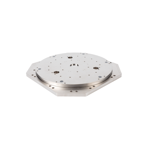
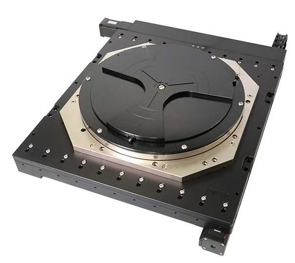
WP120B Low Profile Z Tip and Tilt Stage for 300 mm Wafers
The WP120B is Queensgate’s most accurate wafer positioning stage.
It uses a parallel-kinematic tripod design to achieve sample leveling of ±50 µrad, while achieving milisecond step-and-settle times over the 120 µm closed-loop Z range.
Sub-nanometer-resolution capacitive displacement sensors directly measuring the moving platform, flexure guidance, and high-bandwidth closed-loop control provide exceptional flatness whilst scanning, with pitch and roll errors of less than 2 µrads.
The stage is designed to hold 300 mm wafers, with load capacity up to 8 kg, through-holes allow access for wafer lift-pin systems.
It is compatible with Prior’s ProScan H112 Large Format XY Stage, which offers a full 300 x 300 mm travel range for wafer inspection and defect detection.
| Axis | Z, Tip-Tilt |
| Open Loop Range (Z) | 140 µm |
| Closed Loop Range (Z) | 120 µm |
| Closed Loop Range (Tip Tilt) | 100 µrad |
| Resonant Frequency at 0 kg | 5.2 kg | 8 kg | 320 Hz | 190 Hz | 155 Hz |
| Linearity Error (Z) | Min: 0.06%, Max: 0.15% |
| Linearity Error (Tip-Tilt) | Min: 0.06%, Max: 0.15% |
| Roll Pitch Yaw | 2 µrad (while commanding Z axis only) |
| Step Settle (1 µm) | 9 ms |
| Repeatability, 60 µm step | 5.5 nm |
| Material | Aluminum |
| Stage mass (excluding cables) | 5.8 kg |
| Size (L x W x H) | 375 x 375 x 30 mm |
- Wafer inspection / defect detection
- Electron microscopy (SEM/TEM)
- Interferometry and metrology
- Bonding technology
- Surface structuring
- Wafer probing and chip verification